DELHI : 08 APR 2022
Researchers have computationally designed a low contact resistance metal-semiconductor interface with 2D monolayers for next-generation transistors, which can boost device performance. The discovery of graphene, a flat monolayer of carbon atoms arranged in a 2D honeycomb lattice, has spurred enormous research interest in the materials in the two-dimensional (2D) realm. The lack of resistance in pristine graphene is a major hurdle in its implementation in electronics and switching devices. It cannot control the current flowing through it and cannot switch itself from the ON to the OFF state. Therefore, 2D semiconductors have emerged over time in order to get around the limitations posed by graphene.
Novel properties are observed to arise at the 2D level, which is typically absent in their bulk counterparts. Charge and spin are two well-known properties of an electron. The charge to spin conversion in 2D materials in the presence of interaction of a particle’s spin with its motion or the spin-orbit coupling (SOC) and broken inversion symmetry has opened new avenues in nanoscale study of intrinsic spin of the electron and its associated magnetic moment (spintronics). The strong SOC is a prerequisite for applications in atomically thin spin field-effect transistors.
The modulation in the electronic properties of the materials has turned out to be a boon in improving the device performance by minimizing the metal-semiconductor contact resistance encountered in electronics. A possible way to tune the properties of these monolayers can be paved via external perturbation in the form of small electric field or the application of mechanical strain.
Scientists from the Indian Institute of Nanoscience and Technology (INST), an autonomous institute of the Department of Science and Technology (DST), have suggested new 2D semiconducting monolayers (MgX X=S, Se, Te) having high charge carrier mobility.
The proposed monolayers are unique as they synergistically combine flexibility, spintronic and piezoelectric properties, making them sought after in futuristic self-powered nanoelectronics devices.
The response of these new 2D monolayers to the application of vertical external electric fields can be exploited in electronic devices to store information. The buckled structure with broken inversion symmetry has led to emergence of high out-of-plane piezoelectricity in these monolayers, which can be utilized in generating piezopotential via the application of vertical strain. The piezopotential is capable of regulating the current flow, thereby rendering MgTe monolayer-based devices self-powered. This research published in the journal Nanoscale envisions significant advancement in the field of spintronics and promotes self-powered electronics through the usage of the proposed 2D monolayers.
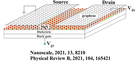
In related research published in Phys. Rev. B, the scientists, Prof. Abir De Sarkar & his Ph.D. Students Manish Kumar Mohanta and Anu Arora have explored low contact resistance between semimetal graphene and MgX. They have found perfect non-resistive contact at the junction of graphene and MgS, a rare and very much sought-after condition for smooth charge transport across the channel. The modulation in electrical contact properties is attained by the application of vertical strain and electric field. This work addresses solutions for very fundamental challenges in pristine graphene — band gap opening via a non-invasive/non-destructive method, stacking dependent contact properties, and tunability of charge carrier concentration. This work can be extended to graphene-based electronic and spintronic devices.
The computational findings are expected to motivate the experimentalists to fabricate futuristic electronic devices, such as piezofield effect transistors, with the desired functionality.

Publications
https://pubs.rsc.org/en/content/articlelanding/2021/nr/d1nr00149c
https://journals.aps.org/prb/abstract/10.1103/PhysRevB.104.165421

 हिंदी
हिंदी


